While single-walled carbon nanotubes (SWCNTs) have found multiple uses in manufacturing, in paints, in plastics, in construction materials and cosmetics, the one sector where it has had the biggest impact is electronics.
However, the development of improved electrical devices that incorporate nanotechnology requires a good supply of pure and inexpensive carbon nanotubes.
Now a combined team from Aalto University in Finland and Nagoya University in Japan have discovered a way to build much cleaner carbon nanotubes ten times faster than current methods. A breakthrough that promises to revolutionise the nanomaterial industry and any product made with them.
Up until now, the market for nanomaterials has been a trade-off between purity and low price. Without clean nanomaterials the quality of an electronic device such as a transparent transistor for a mobile phone screen goes down. Devices work better if they use purer nanomaterial ingredients, but this comes at a price.
As the NASA website explains, “There are several techniques for making carbon nanotubes, all of which require expensive equipment and processes based on the use of metal catalysts.” The problem of achieving good quality carbon nanotubes is that, “These catalysts are difficult to completely remove later on, from the post-production nanotubes, even after cleaning and purification.”
Furthermore, even if good quality carbon nanotubes are purchased (possibly for as much as $1,000 a gram) then the process of using them to make a transistor is slow and dirty. It can take days to convert raw nanomaterial into a transistor, and even then, the chemicals and catalysts used to do so often become attached to the tubes, lowering their purity.
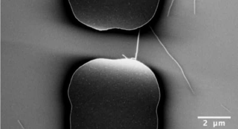
To avoid this contamination, the Finnish/Japanese team led by Prof. Esko I. Kauppinen of Aalto University’s Department of Applied Physics, devised a new approach to making carbon nanotubes for electronic devices using aerosols of metal catalysts and gasses containing carbon. A technique that gave the team much greater control over the fabrication and form of the nanotube structure.
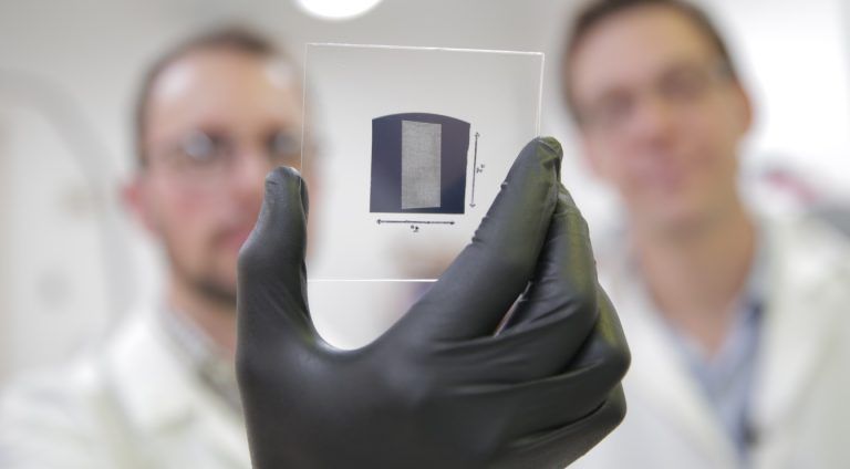
Additionally, the new process makes it possible to synthesize hundreds of individual carbon nanotube transistor devices in less than 3 hours, a ten-fold increase in efficiency.
The researchers have now published their findings “Fast and Ultraclean Approach for Measuring the Transport Properties of Carbon Nanotubes” in the journal of Advanced Functional Materials. Here they explain the process as, “… the fabrication of hundreds of ultraclean field‐effect transistors (FETs) … using single‐walled carbon nanotubes (SWCNTs). The synthesis of the nanomaterial is performed by floating‐catalyst chemical vapor deposition, which is employed to fabricate high‐performance thin‐film transistors. Combined with palladium metal bottom contacts, the transport properties of individual SWCNTs are directly unveiled. The resulting SWCNT‐based FETs exhibit a mean field‐effect mobility which is 3.3 times higher than that of high‐quality solution‐processed CNTs.”

This high field‐effect mobility is in proportion to the cleanliness of the devices, and it is this that most impresses. Whereas other SWCNT transistors experience degradation due to processing attaching chemicals to their surface, these new devices are now called ‘ultra-clean’.
Having such purity in a transistor is further enabling the team to analyse how SWCNTs handle electrons.
“These clean devices help us to measure the intrinsic material properties,” explains Dr Nan Wei, a postdoctoral researcher in the group. “And the large number of devices helps to get a more systematic understanding of the nanomaterials, rather than just a few data points.”

Work is already continuing in both Finland and Japan on how to take commercial advantage of the new method. This includes studying the conducting property of SWCNT bundle transistors as a way to improve the performance of flexible conductive films. The researchers also believe that this could be a route to smash-proof phones and wearable technology.
But it could also just be a way to make cleaner, cheaper carbon nanotubes.