While nanotechnology is today widely used in a variety of industries (electronics, composites, plastics, pharmaceuticals, to name a few) further expansion of the industry has been limited by the technical difficulties of handling such small products.
The manipulation and application of nanowires or carbon nanotubes that can be as small as 1/100th the thickness of a piece of paper is not easy. And if nanoproducts are to realise their full potential in areas such as quantum computing, then improved handling methods will be required.
Understanding that current approaches to nanoproduct fabrication and placement are too bulky and sometimes too corrosive for high-end production, a team from Washington University set about finding a novel way to handle such miniscule objects. The technique they devised can move and control nanowires with lasers.
As the study, which has now been published in the journal Nature Communications, outlines, “As devices approach the single-nanoparticle scale, the rational assembly of nanomaterial heterojunctions remains a persistent challenge. While optical traps can manipulate objects in three dimensions, to date, nanoscale materials have been trapped primarily in aqueous solvents or vacuum. Here, we demonstrate the use of optical traps to manipulate, align, and assemble metal-seeded nanowire building blocks in a range of organic solvents.”
Optical traps (also known as optical tweezers) are a light-based technology which is already widely employed in biology, where it is used to, “operate in a water-free liquid environment of carbon-rich organic solvents, thereby enabling new potential applications.”
By using optical tweezers, which act as a light-based ‘tractor beam’, the team can more precisely assemble nanoscale semiconductor materials, putting the pieces together to form larger, more powerful structures.
“This is a new approach to nanoscale manufacturing,” says Peter Pauzauskie, the study’s senior co-author and a UW associate professor and faculty member at the Institute for Nano-engineered Systems. “There are no chamber surfaces involved in the manufacturing process, which minimizes the formation of strain or other defects. All of the components are suspended in solution, and we can control the size and shape of the nanostructure as it is assembled piece by piece.”
Beyond improved control of the nanoproducts, the new method also protects their integrity. As co-senior author Vincent Holmberg, a UW assistant professor of chemical engineering and a faculty member at the Molecular Engineering & Sciences Institute, explains, “Using this technique in an organic solvent allows us to work with components that would otherwise degrade or corrode on contact with water or air. Organic solvents also help us to superheat the material we're working with, allowing us to control material transformations and drive chemistry.”
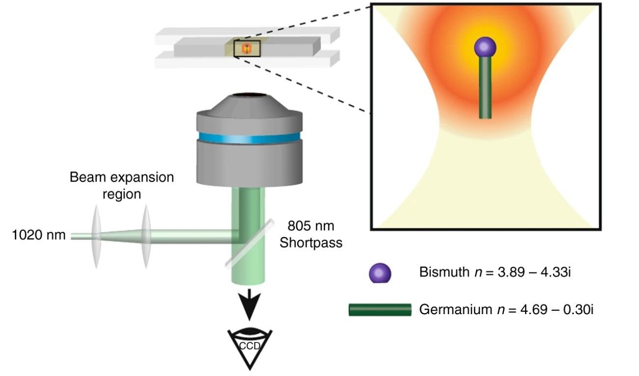
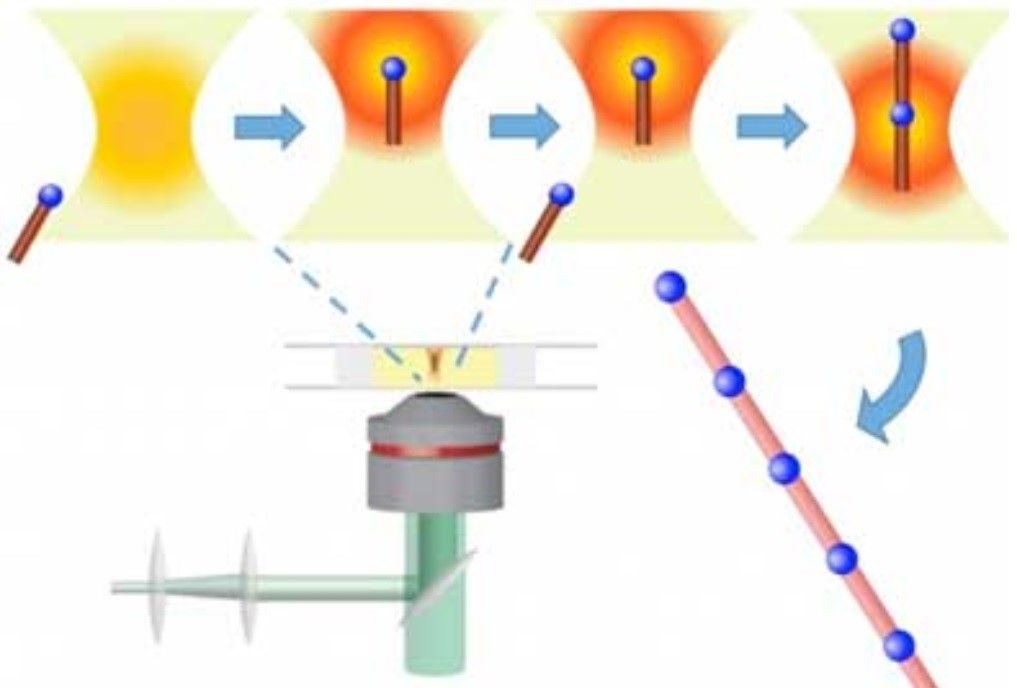
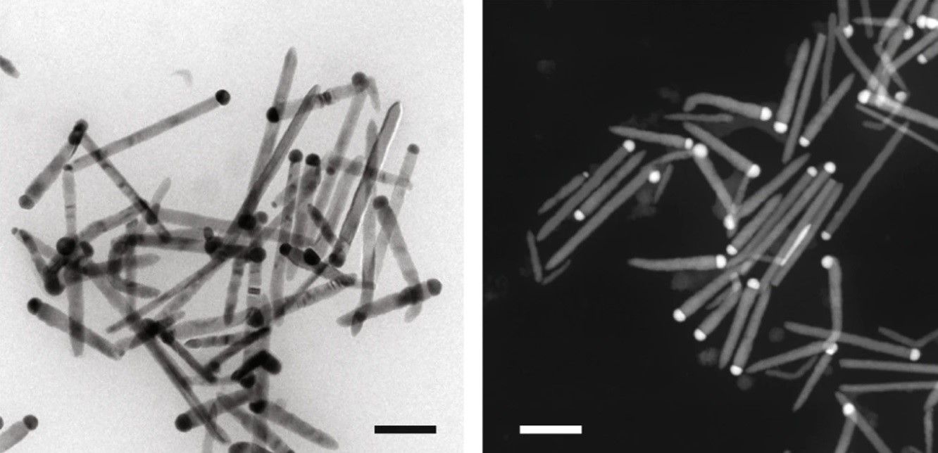
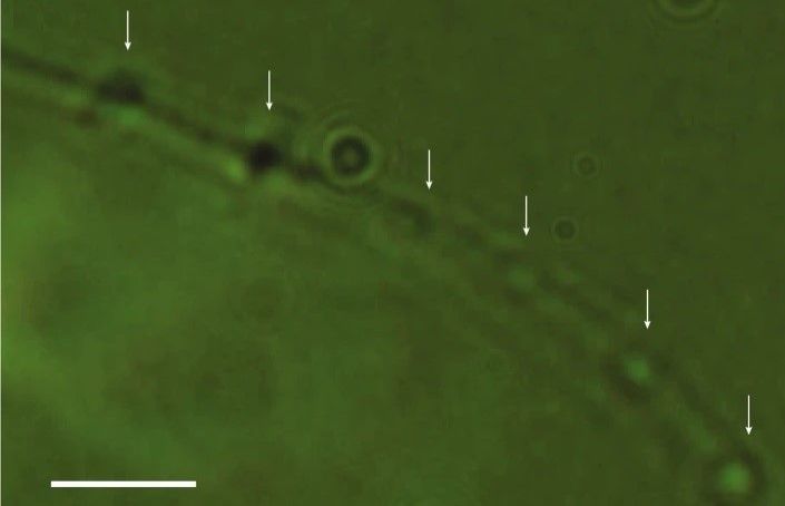
Describing the process, the University of Washington press release explains that, “To demonstrate the potential of this approach, the researchers used the optical tweezers to build a novel nanowire heterostructure, which is a nanowire consisting of distinct sections comprised of different materials. The starting materials for the nanowire heterostructure were shorter ‘nanorods’ of crystalline germanium, each just a few hundred nanometers long and tens of nanometers in diameter — or about 5,000 times thinner than a human hair. Each is capped with a metallic bismuth nanocrystal.”
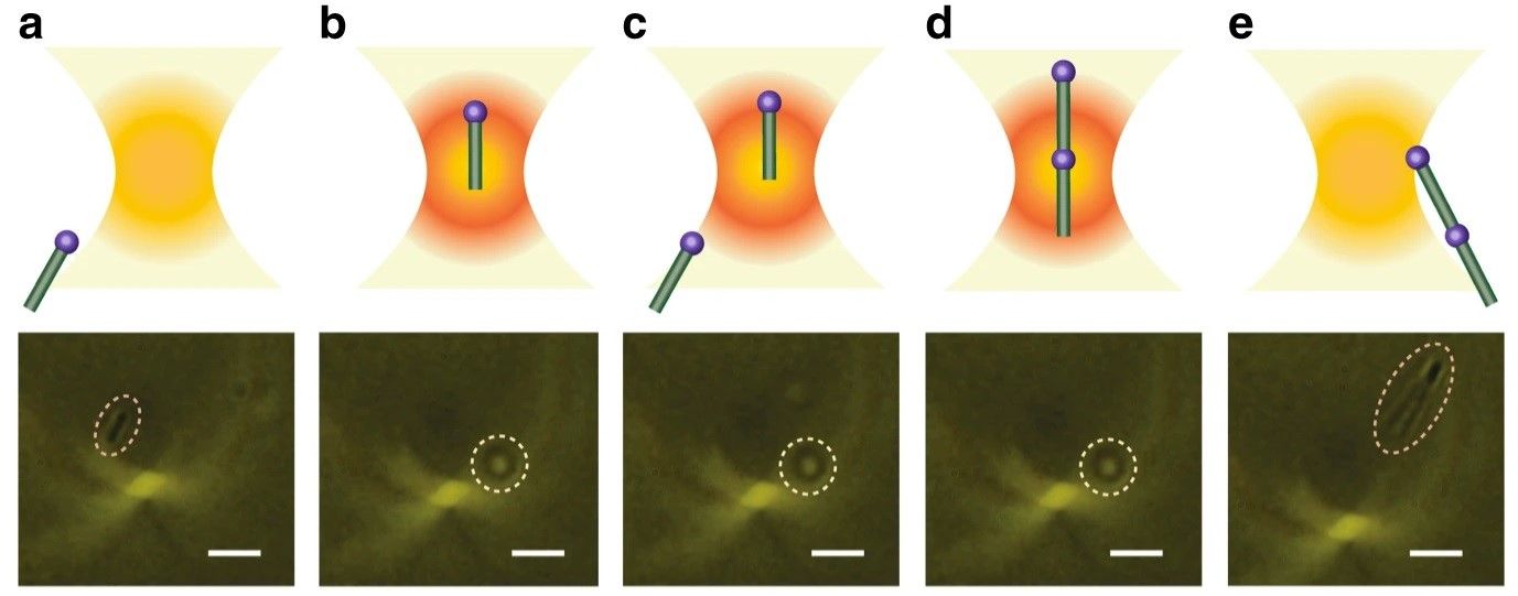
The light-based ‘tractor beam’ was then used to grab one of the germanium nanorods. As the energy from the beam superheats the nanorod, the bismuth cap melts, allowing a second nanorod to be attached to the molten end. Both nanorods have then been soldered together, both were manipulated into place by the ‘laser’.
By repeating the process, the researchers were able to assemble, “a patterned nanowire heterostructure with repeating semiconductor-metal junctions that was five-to-ten times longer than the individual building blocks”.
“We've taken to calling this optically oriented assembly process ‘photonic nanosoldering’, says Holmberg, “essentially soldering two components together at the nanoscale using light.”
Such is the precision of the optical trap that in effect single germanium nanorods are being captured, guided, and released by the power of the photons that make up the laser beam. A force that is highly adjustable allowing for such detailed nanoscale manufacturing.
“This is the kind of precision needed for reliable, reproducible nanofabrication methods, without chaotic interactions with other surfaces or materials that can introduce defects or strain into nanomaterials,” says Pauzauskie.
Alongside their nanosoldering approach, the team believe that the improved method of handling nanoscale materials could enable additive manufacturing of nanoscale structures by using different materials for different applications.
One such application, may be in the development of quantum computing. As the nanowires are connected in sections that could consist of different materials, it is possible that a composite nanorod could provide a route to creating topological qubits, the computational points in advanced computers. Other uses include single-particle catalysis, additive nanomanufacturing from constituent nanomaterial building blocks, or future hydrodynamic studies.
“We hope that this demonstration results in researchers using optical trapping for the manipulation and assembly of a wider set of nanoscale materials,” said Holmberg, “irrespective of whether or not those materials happen to be compatible with water.”
It may also herald a new era in nanotechnology, allowing for improved manipulation of nanotubes, graphene, and nanowires. Removing a further barrier to allow the nano-production industry to take off – in both a big and a very small way.