Silicon, the raw material that has supported the electronics industry for the past six decades, is at the end of its lifespan. A new material for electronics is needed, and it could well be a 2D nanomaterial form of antimony.
The need for a new substance for next generation electronic devices is based on the basic principle on how transistors work, a function that is increasingly restricted by Moore’s Law.
Technology Review explains this as follows; “Moore’s Law is named after Intel cofounder Gordon Moore. He observed in 1965 that transistors were shrinking so fast that every year twice as many could fit onto a chip, and in 1975 adjusted the pace to a doubling every two years.”
Since then, the law has held true. In the year 2000 the number of transistors in a mid-range CPU numbered 37.5 million, while in 2009 the number grew to 904 million - a four-and-a-half-fold increase.
More recently, the doubling effect has begun to slow down. This is because of the physical limitations of how small a silicon transistor can physically be, how many can fit on a microchip, and at what price.
Consequently, the electronics industry has focused on improving performance in other ways, such as multi-core processing. In turn, Moore’s Law has often been adapted to reflect a doubling of computing speed, instead of a straight transistor count.
Despite this, the law is reaching its limit, as the physical properties of silicon are reaching their limit.
It is one of the biggest challenges facing the technology industry, and a team for engineers from the University of Texas at Austin may have found the solution; a new material for manufacturing even smaller computer chips by replacing silicon.
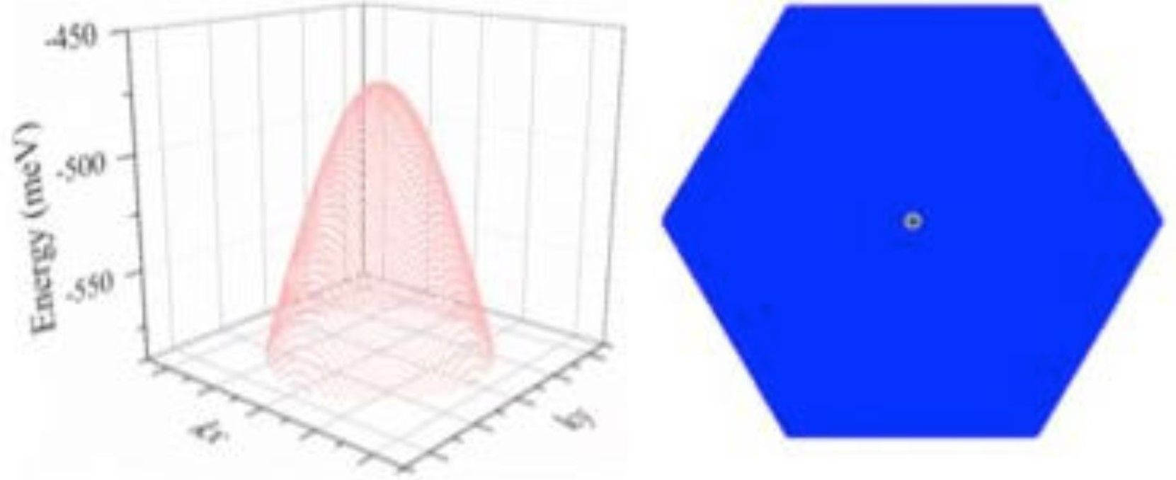
The study was based at the Cockrell School of Engineering, where Yuanyue Liu, an assistant professor and member of UT's Texas Materials Institute, and his colleagues were looking at silicon and its semiconductor properties. They noticed that the while the electrons moved quickly through the material, they also scattered in many directions.
Analysis of the chemical element antimony in its 2D form found the electrons, as the nanotechnology journal Nanowerk describes, “… could be made to move together in an orderly way, giving it high charge mobility and making the material an efficient semiconductor.” A discovery that may lead to the electronics industry converting from silicon to a nanomaterial form of antimony.
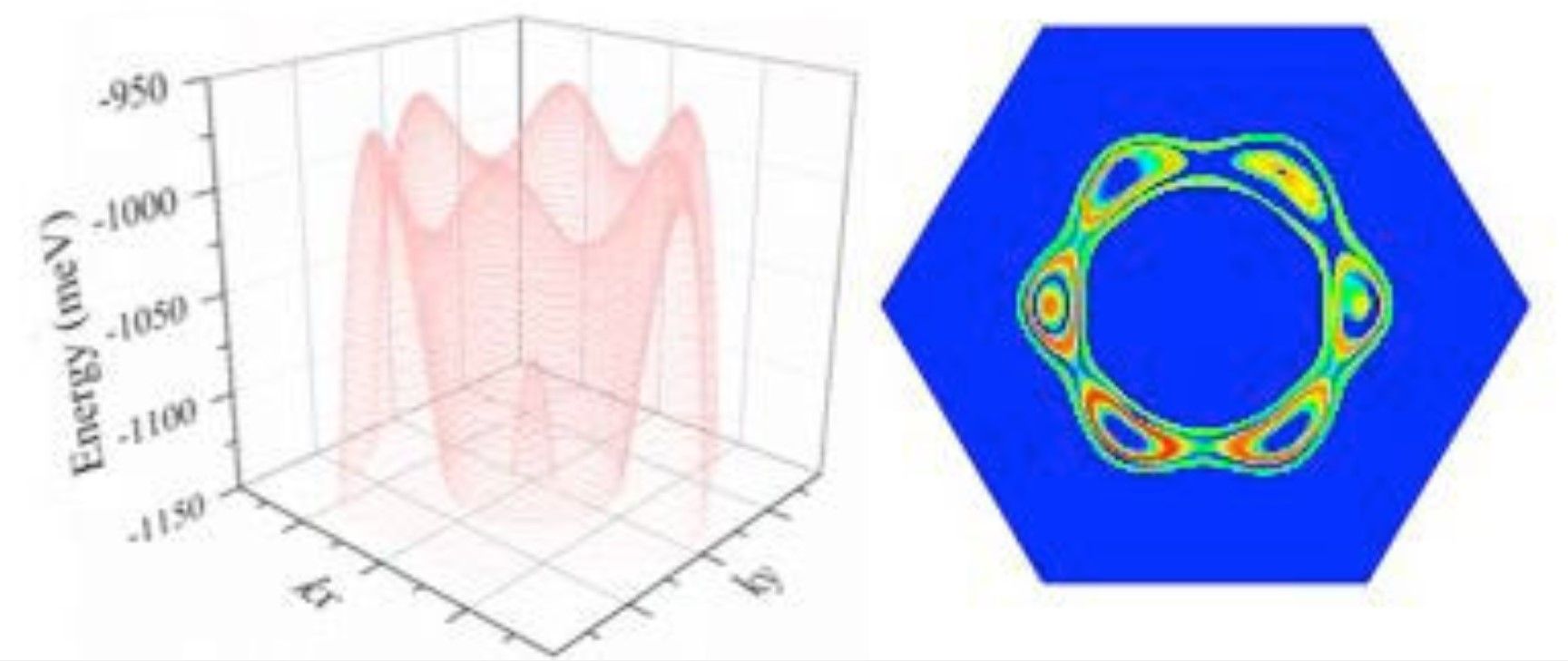
As the university press release, explains, “Antimony is a semi-metal that is already used in electronics for some semiconductor devices, such as infrared detectors. As a material, it is only a couple of atomic layers thick and has a high charge mobility - the speed a charge moves through a material when being pulled by an electric field. Antimony's charge mobility is much higher than other semiconductors with similar size, including silicon. This property makes it promising as the building block for post-silicon electronics.”
The study has now been published in the Journal of the American Chemical Society.
While at present, Liu’s work on using 2D materials to replace silicon has only been demonstrated through theoretical computational methods, the team is confident that nanoscale antimony will retain the same properties in practice. Consequently, the team have begun conducting physical tests and plan to publish this study shortly.
Meanwhile, the theoretical analysis of how 2D antimony operates is continuing, as the researchers hope to find further ways that nanomaterials can advance technology. Beyond replacing silicon in transistors, does this nanomaterial discovery have broader significance?
“Most importantly,” notes Liu, “we have uncovered the physical origins of why antimony has a high mobility. These findings could be used to potentially discover even better materials.”
It seems that nanomaterials may soon provide a replacement for raw materials everywhere.
Photo credit: Nanowerk, Troyewelch, Economist, & Arstechnia