An international team of nanospecialists have developed a soft nanocomposite electroadhesive (SNE), that will enable the manufacture of ever smaller electronics. By supplying a forest of carbon nanotubes with an electric charge, the researchers have found a workable way to pick up and place objects measuring as small as 20 nm in diameter, breaking current limitations that prevent the construction of nanoscale devices.
Using current technology, manufacturers of high-end miniature electronics have reached the limit on making circuits any smaller. Mechanical sensors and accelerometers can be made that are smaller than 1 mm. While integrated circuit (IC) chips for radio-frequency communication can be one tenth of a millimetre or smaller, and micro–light-emitting diodes (LEDs) for next-generation displays are smaller still, measuring only 1 to 10 micrometres in width.
The challenges in making electronics beyond these limits were outlined in the study (published in the journal Science Advances), stating that, “At present, automated pick-and-place assembly is the benchmark technique for the manufacturing of circuit boards and the integration of miniature ICs into systems-on-chip. However, despite advances in miniature robotic grippers and vacuum nozzles, manipulation is increasingly challenging as object size decreases, because gravity forces diminish more rapidly than van der Waals forces or electrostatic attraction. Intricate micromechanical grippers suffer from stiction [static friction that needs to be overcome to enable stationary objects to lift off from a surface] and therefore cannot reliably place microscale objects without the aid of secondary adhesive surfaces.”
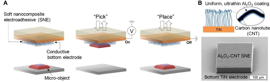
What is required is a technique or device that can repeatedly switch between strong adhesion for picking objects up, and weak adhesion for placing objects down. Due to the level of control required at this scale and the delicate nature of handling such small parts, any solution to this problem would ideally not involve heating, shearing, or chemical reactions.
Now the study from MIT, the Korea Advanced Institute of Science and Technology, and the University of Pennsylvania, have made a breakthrough by varying the voltage applied to a loose forest of carbon nanotubes. In doing so, the researchers were able to easily switch on and off an adhesive force, making a practical method for the lifting and placing of both metal and dielectric nanoscale bodies.
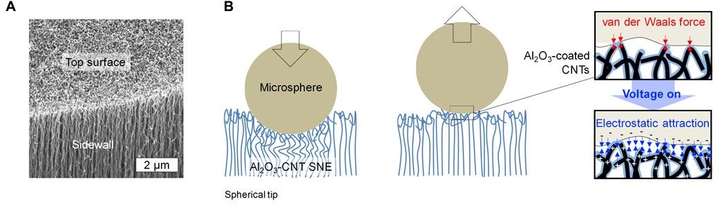
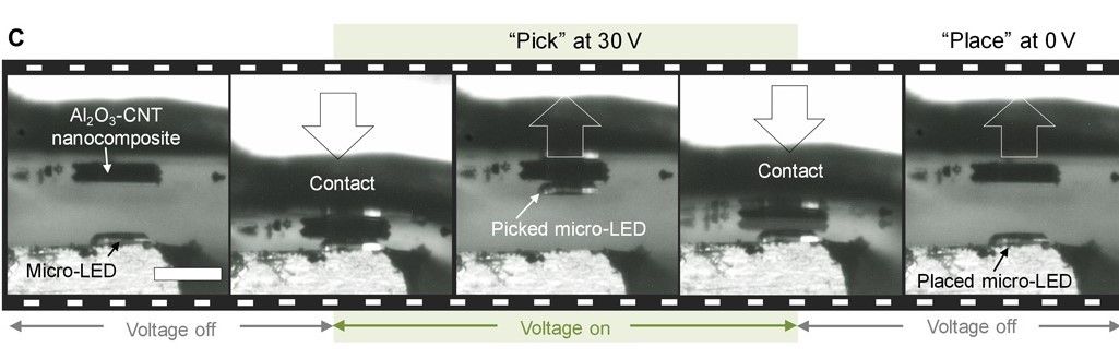
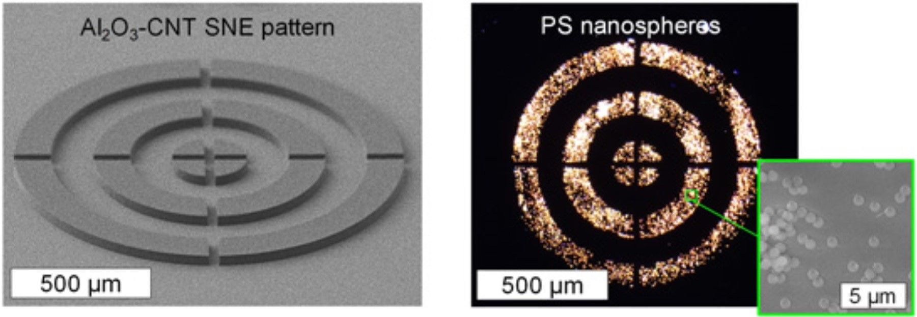
As the scientific journal Nplus One, reports, “The application of electric voltage temporarily polarizes the dielectric shell of nanotubes, which increases the adhesion by electrostatic, more than a hundredfold. As a result, a forest of nanotubes, which is normally about 40 times less ‘sticky’ than most other solids, forms a much stronger bond when 30 volts are applied. The corresponding experiments measured a force of 2.3 micronewtons for an area measuring 200 by 200 microns.”
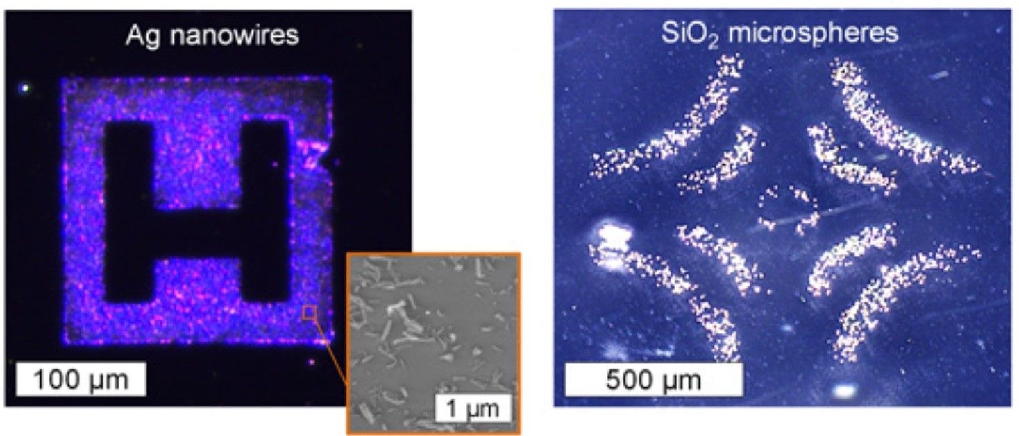
This force enabled the team to pick up and place films of silver nanowires, as well as metal and polymer microparticles, and light-emitting diodes measuring 170 μm by 170 μm by 50 μm.
Up until now, the lifting and letting go of such small items was beyond the capabilities of modern mechanical manipulators, which at present struggle to move objects that measure less than 50 microns. The smallest items that the team were able to pick up and place with the carbon nanotube method measured only 20 nanometres.
While the technique of electroadhesion is already in use for moving larger bodies such as silicon wafers or fabrics, this is the first time it has been applied to nanoscale objects. But with modern electronic components shrinking to the size of grains of flour, a breakthrough in moving and placing these parts was needed.
This work has now made further advances in electronics possible by using soft, nanostructured surfaces to manipulate metallic and dielectric objects without thermal or chemical adhesion.
As well as enabling the improved production of nanoscale electronics, the method may also find applications in biotechnology, optoelectronics, and energy conversion systems.
Photo credit: Science Advances & Lifeboat