Nanowires have many applications in industry. They are used in miniaturized photonic and electronic components, such as optical circuits on chips; as novel biological and chemical sensors; and play an important role in quantum computing.
But their range of uses could be further extended if their ability as extremely small semiconductors included transforming electric energy into light energy and vice versa, at the correct wavelengths. This would greatly improve their potential in solar panels, making them much more efficient, and would also make them a raw material for LEDs, giving them colour.
Now a team from the research centre at Helmholtz-Zentrum Dresden-Rossendorf (HZDR) claim they have achieved this crucial step by a process that manufactures nanowires with operating wavelengths. By simply modifying the structure of the nanowire’s shell the researchers are able to select the wavelength desired, dramatically expanding the number of applications for this revolutionary nanoproduct.
The team has now published its results in the journal Nature Communications, where they explain how they have discovered, “… unique opportunities for strain engineering in nanowires to achieve wide tuning of the bandgap… .”
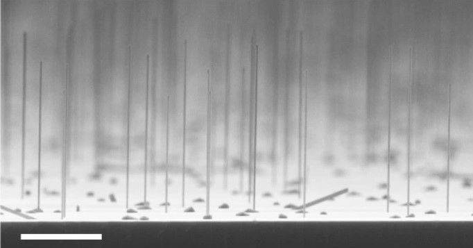
The breakthrough came after years of experimentation synthesizing nanowires from gallium arsenide (a semiconductor material) on silicon substrates. This led them to explore the idea that by altering the materials’ mismatched crystal structure they could promote a mechanical strain on the core of the nanowire. This strain would induce new electronic characteristics on the gallium arsenide semiconductor material.
The logic behind this is described by the industry journal Nanowerk, which explains that as, “… a semiconductor bandgap becomes tinier, the electrons become more mobile. To amplify this effect, the researchers continued to add more amounts of indium to the shell or alternatively increased the thickness of the shell. The outcome went far beyond expectations.”
“What we did was take a known effect to extremes,” notes Dr Emmanouil Dimakis, the study’s lead author.
What they had expected was for the nanowire to bend or distort, or some similar defect to occur. But instead, the scientists saw that a higher strain allowed for the bandgap for the nanowire semiconductor to be moved to ‘extremely low energies’.
Previously, to reach such a low spectral range, unique alloys (such as indium) were used. However, employing these alloys created other problems due to the mix of material, and so they were generally deemed unsuitable. By using a gallium arsenide structure, the researchers have solved the challenge in a completely unexpected way.
“The reason for the absence of such disorders can be attributed to the unique experimental commotions,” explains the industry journal Azonano. “The researchers initially grew very thin gallium arsenide wires, which were about five thousand times finer than a human hair. Next, they managed to create a wire shell at extraordinarily low temperatures. By then, surface diffusion of atoms is more or less frozen, causing the shell to grow uniformly around the wire core.”
As Dimakis observes, “Scientists have been aware of gallium arsenide as a material for years, but nanowires are special. We shifted our focus to the question of what triggers the extremely high strain in the nanowire core, and how this can be used for certain applications.”
The fact that nanowire semiconductors can operate at such low energies is a true breakthrough. They can now even be used in fibre-optic networks, which is in itself a milestone for the nanowire industry.
But in many ways, this discovery merely opens the door for other researchers to expand on how nanowires with tuneable wavelengths can be developed and applied across industry. Whether they will result in more efficient solar cells, colourful LEDs, or some other as yet thought of application remains unclear.
However, the fact that nanowires semiconductors can be manufactured with tuneable wavelengths shows how strange and yet profitable the nano-industry can be.
As Dimakis summarises, “A material may exhibit completely new properties at the nanoscale.”
Photo credit: HZDR/René Hübner, & ABC,
