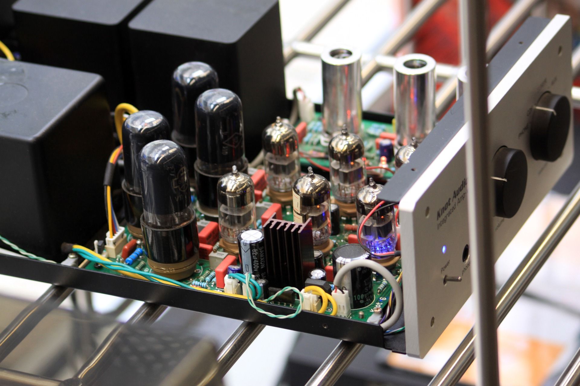
Early electronics were extremely dependent on vacuum transistors as both amplifiers and switches. Their high speed and immunity to noise made them a practical solution for the technology required at the time. However, they suffered from several major disadvantages, including high energy consumption, short tube lifetime, and large size.
As a result, by the 1970’s they had been almost entirely replaced by semiconductor transistors.

But now, vacuum transistors may be about to make a comeback, as a team of researchers from the NASA Ames Research Center have shown that nanoscale vacuum channel transistors (NVCTs) can be synthesized on silicon carbide wafers making them a viable alternative to solid-state transistors.
The use of NVCTs eliminates the problem of size. Whereas traditional vacuum tubes have the shape tiny light bulbs, the nanoscale tubes are miniscule. While the researchers grew their sample on a 150mm wide silicon carbide wafer, the transistors themselves measure only a few nanometres wide and can only be seen under a scanning electron microscope. Their improved gate structure has also lowered energy consumption from 10 volts to less than five.

The discovery is best described by the scientific journal Phys.org, which explains that, “In an NVCT, the gate is the component that receives the drive voltage and, based on this voltage, it controls the flow of electrons between two electrodes. In contrast, in the old vacuum tubes, electrons were released by heating the emitter of the device. Because the electrons travelled through a vacuum (the vacuum gap), they moved at very high speeds, which led to the fast operation.”
Adding that, “In NVCTs, there is not actually a vacuum, but instead the electrons travel across a space filled with an inert gas such as helium at atmospheric pressure. Since the distance between electrodes is so small (as little as 50 nm), the probability of an electron colliding with a gas molecule is very low, and so the electrons move just as quickly through this ‘quasi-vacuum’ as they do in an actual vacuum. Even with some collisions occurring, the gas molecules are not ionized due to the lower operating voltage.”

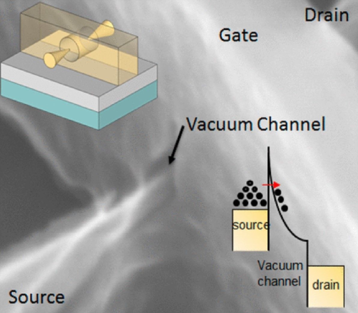
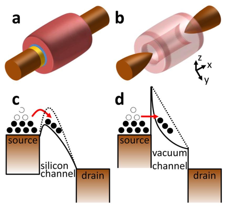
This is a significant breakthrough, especially as NVCTs can be used as a direct swap for solid-state transistors inside current circuitry. The team has already begun testing electronic devices that have been made using an identical process to that used in manufacturing circuits with standard MOSFETs (metal oxide semiconductor field-effect transistors). The only difference being that the semiconductor channel, which in MOSFETs is placed between the source and the drain, has been replaced with an empty channel.

As the study’s lead author, Jin-Woo Han explains, “We have fabricated sub-100 nm feature scale vacuum channel transistors in both silicon and silicon carbide material systems. The implication is that we can use our current manufacturing infrastructure and known material systems to make ultra-small vacuum devices.” Adding that, “Their performance is encouraging, and the transistors are not affected by radiation.”
While radiation may not be a problem for most devices, it is a major challenge in extreme locations.
“Off-the-shelf-electronics have very little use for space missions because of the impact of radiation,” notes Meyya Meyyappan, one of the study’s researchers. “Typically, radiation-shielding or advanced radiation-aware circuit design would be needed, all of which are expensive, time consuming and result in hardware that is not the state-of-the-art. We have combined the best of vacuum physics and modern integrated circuit manufacturing to produce nanoscale vacuum transistors to overcome the above shortcomings.”
Alongside their tolerance for ionizing radiation, NVCTs have also been shown to work at the same performance level in temperatures of up to 200°C, a heat at which standard transistors would fail. They have also been found resistant to both proton and gamma radiation, and so could be ideal candidates for other extreme environments that use terahertz electronics and other high-frequency devices.
Tests have also shown that silicon carbide devices (onto which the NVCTs are synthesized) can increase long-term stability, making them even more suitable for hard to replace electronics.
While such nanoscale technology may sound expensive and only economic in specialized circumstances, there are clear benefits to be had in further developing NVCTs. As an NASA Ames Research Center study published in the journal Nano Letters, outlines, “The nanoscale vacuum channel transistor is a possible alternative to semiconductor transistors beyond Moore’s law - which states that the number of transistors on a computer chip doubles approximately every two years. This is soon expected to hit a roadblock due to the physical limitations of shrinking semiconductor transistors.”
As Meyyappan notes, “Since the channel has nothing, electrons can be faster than in semiconductors where they experience scattering with the lattice, and thus the operating frequency or speed can be higher.”
NASA has now filed for a patent of this technology, and have outlined how the nanomaterial design of old technology could have uses not only in space communication and exploration, but also in satellites, biosensors, analysis of light at a nanoscale (nanophotonics), and biomedical technology.
Photo credit: Phys.org, Nanoletters, Eenewseurope, Wikipedia, Sciencemag & Klabs
