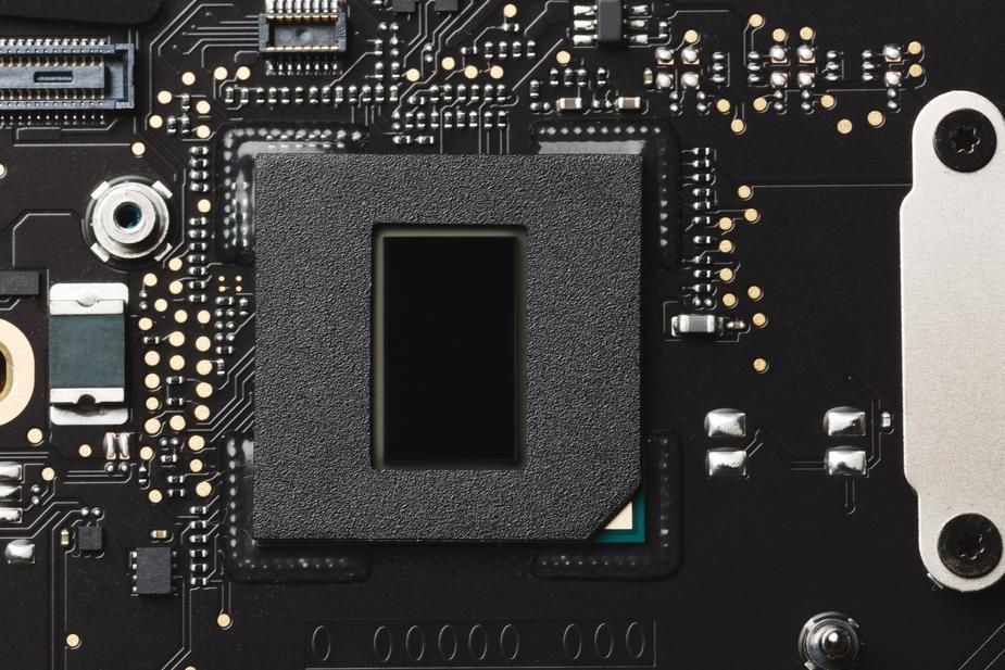
In the world of ever-smaller electronic devices, manufacturers of computer processors are hitting a wall. While they have been able to shrink the size of electronic parts year-on-year for the past five decades they are now reaching the limits of the laws of physics when using silicon.
One possible way to make much smaller processors is by using carbon nanostructures.
Based on its size and shape, graphene is both thermally and electrically conductive (or semi-conductive). It also has the additional properties of being flexible, tear-resistant, lightweight, strong, versatile, and only two-dimensional, and so makes for an ideal raw material for minute electronic devices. This means that it could replace copper (which is conductive) or silicon (which is semi-conductive) in the manufacture of nanotransistors and processors.
The challenge facing designers of ultra-small electronic devices is that carbon nanostructures (such as nanotubes) are typically formed on metallic surfaces. As the nanotechnology industry journal Nanowerk, explains, carbon nanotube (CNT) manufacturers use a process called chemical vapor deposition (CVD) to make carbon nanotubes as it, “… allows the production of larger quantities of CNTs under more easily controllable conditions and at lower cost. In the CVD process, manufacturers can combine a metal catalyst (such as iron) with carbon-containing reaction gases (such as hydrogen or carbon monoxide) to form carbon nanotubes on the catalyst inside a high-temperature furnace.” However, the resulting ‘forest’ of CNT’s are “… adhered to a synthesis substrate which is typically stainless steel or copper foils.”
As the scientific journal Science Daily explains, “In order to create an electronic circuit, the molecules of nanographene must be synthesised and assembled directly on an insulating or semi-conductive surface. Although metal oxides are the best materials for this purpose, … direct synthesis of nanographenes on metal oxide surfaces is not possible as they are considerably less chemically reactive. The researchers would have to carry out the process at high temperatures, which would lead to several uncontrollable secondary reactions.”
However, in the last month, a research team funded by the German Research Foundation (DFG) has discovered a process that forms carbon nanostructures on metal oxide surfaces, paving the way for their use in electronic devices.
The breakthrough process was explained on the Friedrich-Alexander-Universität Erlangen-Nürnberg (FAU) website, where they describe how, “The researchers’ method involves using a carbon fluorine bond, which is the strongest carbon bond. It is used to trigger a multilevel process. The desired nanographenes form like dominoes via cyclodehydrofluorination on the titanium oxide surface. All ‘missing’ carbon-carbon bonds are thus formed after each other in a formation that resembles a zip being closed. This enables the researchers to create nanographenes on titanium oxide, a semi-conductor. This method also allows them to define the shape of the nanographene by modifying the arrangement of the preliminary molecules. New carbon-carbon bonds and, ultimately, nanographenes form where the researchers place the fluorine atoms.”
While the process requires many steps, the researchers believe that they have found a practical way to apply nanostructures in everyday electronics. As their results, now published in the journal Science, outline, “The high efficiency of a hydrogen fluoride ‘zipping’ makes our approach attractive for the rational synthesis of nanographenes and nanoribbons directly on insulating and semiconducting surfaces.”
“This ground-breaking innovation offers effective and simple access to electronic nanocircuits that really work,” says Dr Konstantin Amsharov, the research group’s leader. While further research will be required to confirm that mass production is feasible, it seems that the team have found a revolutionary way to make smaller electric transistors, processors, and ultimately electronic devices. As Amsharov states, if it all goes as expected, “[We] could scale down existing microelectronics to the nanometre scale.”
Photo credit: Cheaptubes, NagoyaUniversity, FAU, Noisebreak, & Edgefx