One of the biggest challenges for the newly born nanotechnology industry has been the ability to grade its products. Most industries have standardized methods of evaluating the good from the bad. Eggs are graded on size, shape, and shell strength; diamonds on carat, cut, clarity, and colour, concrete on its mix ratio (sand:cement:aggregate) and its compression strength.
But grading products for which you need an electron-microscope to see isn’t so easy.
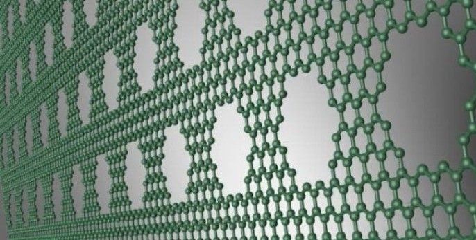
As nanoproducts, such as nanotubes, buckyballs, nanowires, and nanosheets like graphene are synthesized or ‘grown’ the number of flaws in the them can vary greatly from one producer to the next. The number of unwanted holes in a sheet of graphene can seriously impact how effective the nanomaterial is as a product, reducing its strength, flexibility, and/or electroconductivity.
But how to grade the good products from the bad?
How can the nanotechnology industry grade good-quality graphene?
The answer it seems was clear all along. This is because a team of researchers from the U.S. Department of Energy’s Ames Laboratory have found a way to detect near-flawless graphene using low energy electron diffraction.
“The discovery is a paradox,” said Michael Tringides, a senior scientist at Ames Laboratory whose work involves analysing the unique properties of 2D materials. “Textbook diffraction states that the more flawless a material is, the sharper and clearer the diffraction spots, and imperfect materials have low intensity, broader diffraction spots.”
Unexpectedly, diffraction studies of high-quality graphene, with a good uniformity of structure, showed not only sharp spots, but also a very wide band of diffuse diffraction in the background.
Materials used at the nanoscale (1mm = 1 million nanometres) have different properties and special advantages over those used in bulk.
For example, a gold bar must be heated to 1,064oC before it starts to melt. But the same gold bar in nanoform will melt at 591oC.
Similarly, gold (as an inert material that doesn’t corrode or tarnish) would normally be considered a bad choice of material to use as a catalyst for chemical reactions. However, at a scale of 5 nanometres it can act as a catalyst for a reaction such as oxidizing carbon monoxide.
Nanotechnology enables engineers to do things that were previously impossible, giving it real-world, practical uses.
“That result is not intuitive and very strange,” notes Tringides, “but we find this broad diffraction pattern to be an intrinsic feature to graphene, and when you have it, you have very good graphene. This is a good way to quantitatively measure its structural perfection.”
The study’s findings have now been published in the APS Physics journal, Physical Review B.
Astoundingly, the way that quality graphene produces a broad diffraction pattern was visible since it was first created 25 years ago, yet no one acknowledged its presence. The ability to grade graphene in this way was simply ignored.
Only now have nanospecialists recognized the significance of this trait. As Tringides says, “It was a big, noticeable phenomena, and reproducible, and we realized it must be extremely important in some way.”
Exactly why graphene has this property is not fully known, however some theories are already being investigated. As the nanotechnology journal Nanowerk, explains, “… scientists believe the broad diffraction phenomenon is caused by the confinement of graphene electrons within a single layer of atoms. According to the fundamentals of quantum mechanics, because the electron position normal to the layer is precisely known, their wave vector must have a spread, which is transferred to the diffracted electrons.”
What is understood, is how this discovery will further advance the nanotechnology industry. Not only by enabling simpler trade in nanomaterials, but also in developing improved nanoproducts.
“This effect is significant for other types of 2D materials as well,” notes the journal. “With the continued and growing interest in 2D materials for a variety of applications, improving their structural quality will be the key to promising new technologies.”
As Tringides concludes, “This work provides an important step towards the ability to optimize graphene and other 2D materials precisely, and tailor their properties for specific applications.”
Photo credit: Singularityhub, Phys.org, Semanticsscholar, & Azosensors